Device Nanofabrication
I have extensive hands-on experience designing and fabricating gate-tunable nanoscale devices through a fabrication workflow that involves numerous interdependent steps, including exfoliation and stacking of 2D materials, photolithography, metal deposition, etching, and AFM-based nanofabrication. My expertise lies in designing devices that are engineered specifically for in-operando microscopy, where surface sensitivity, contact resistance, and electrostatic control require rethinking conventional fabrication recipes. My fabrication process is inherently iterative: device testing directly informs subsequent design and process modifications, leading to steady improvements in device performance.
I made a brief animation to illustrate the fabrication workflow for making a gate-tunable moire field-effect transistor compatible with in-operando scanning tunneling microscopy.
Fabrication Workflow
Exfoliation and identification of 2D flakes from bulk crystals (graphene, hBN, TMD).
AFM nanolithography may be performed on specific flakes (usually graphite) to etch special flake geometries with nanometer precision.
Mechanical stacking of flakes using PVC / PDMS stamp. The stack is covered by a sacrificial few-layer hBN flake that is removed after lithography. The purpose of this flake is to protect the device’s surface during subsequent processing steps. The stack is released on an Si/SiO2 substrate (Figure 1).
Photolithographic or electron-beam patterning of contact pattern.
Metal evaporation of contacts.
Removal of sacrificial hBN (Figure 2).
“Scratching” of exposed surface using contact-mode AFM to “sweep” away left-over residue.
The device is mounted on a sample-holder and wire-bonded to macroscopic contact pads.
Ambient testing of electrical contacts.
Ultra-high vacuum anneal.
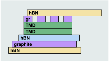
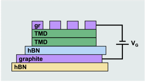
Figure 1: Schematic of a generic 2D heterostructure before (left) and after (right) the sacrificial hBN is removed.
Figure 2: A live video of the hBN sliding process. The polymer stamp (left) latches onto the sacrificial hBN layer and drags it off of the device stack.
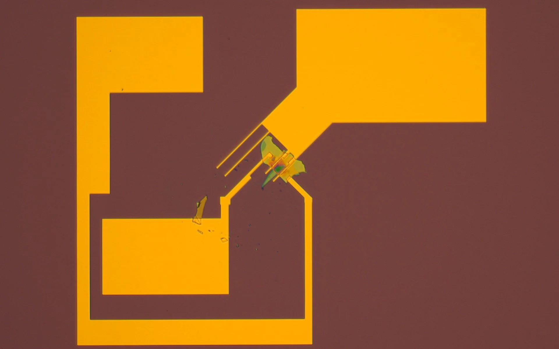
Optical image of an inter-leaved dual split gate twisted WSe2 device.
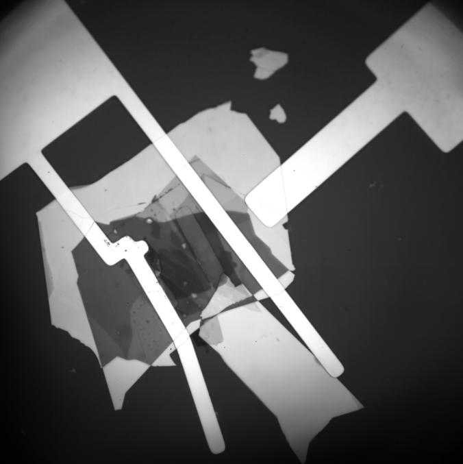
Optical image of a RuCl3 + contact gate twisted WSe2 device, designed to have low contact resistance.
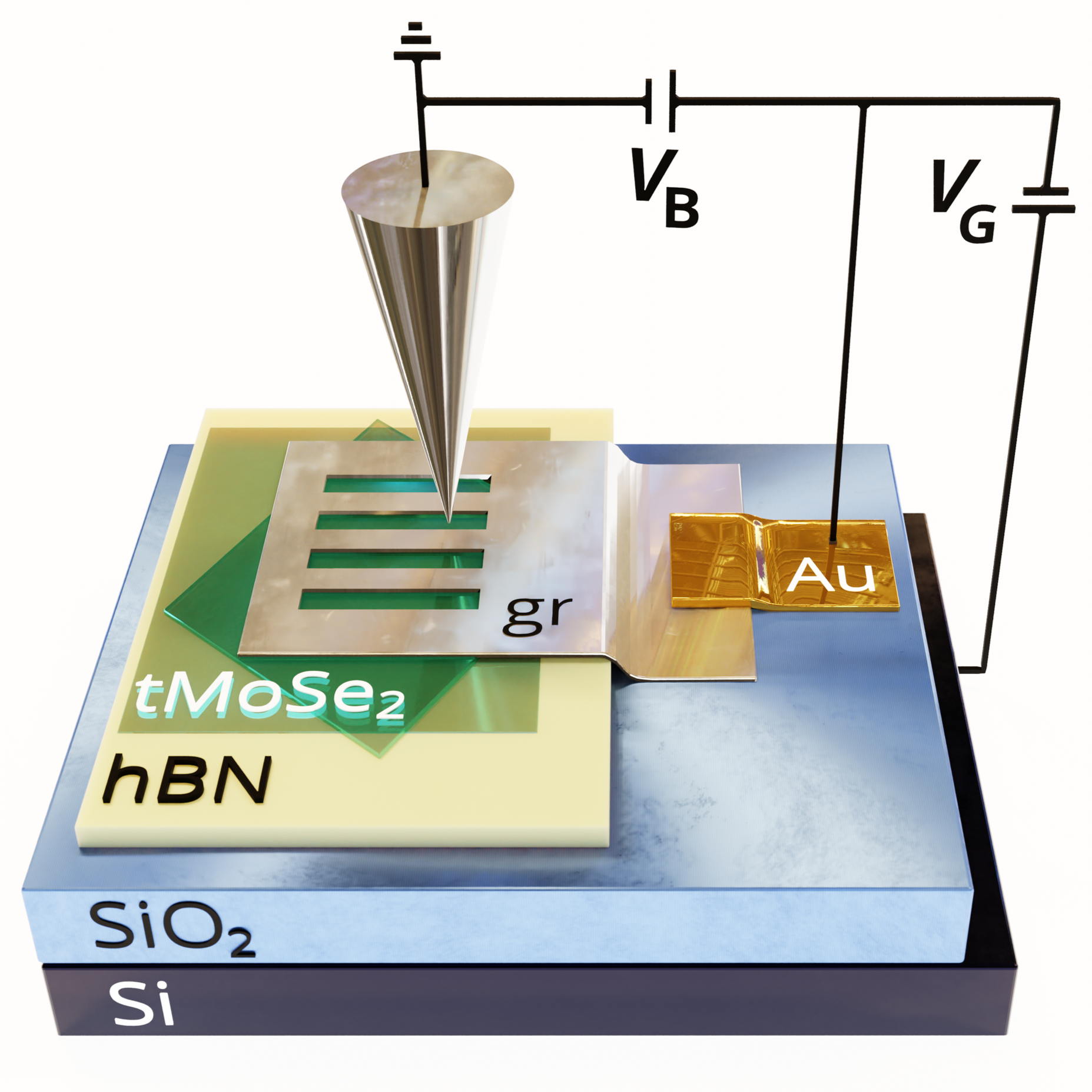
Schematic of a basic twisted MoSe2 device with a Si back-gate for STM investigation.