In-operando Scanning Tunneling Microscopy
I use in-operando scanned probe microscopy, including scanning tunneling microscopy (STM) and atomic force microscopy (AFM), to directly visualize electronic wavefunctions in solid-state materials with atomic resolution. In STM, a sharp metallic tip is positioned within a nanometer of a conductive surface, allowing electrons to quantum mechanically tunnel across the gap. By scanning the tip and measuring variations in the tunneling current, the local electronic structure of the material can be mapped with atomic-scale precision. These measurements are typically performed at cryogenic temperatures (< 4 K) in an ultrahigh-vacuum environment.
I specialize in state-of-the-art in operando measurements that visualize electronic wavefunctions in nanoscale devices as device parameters are tuned in situ.
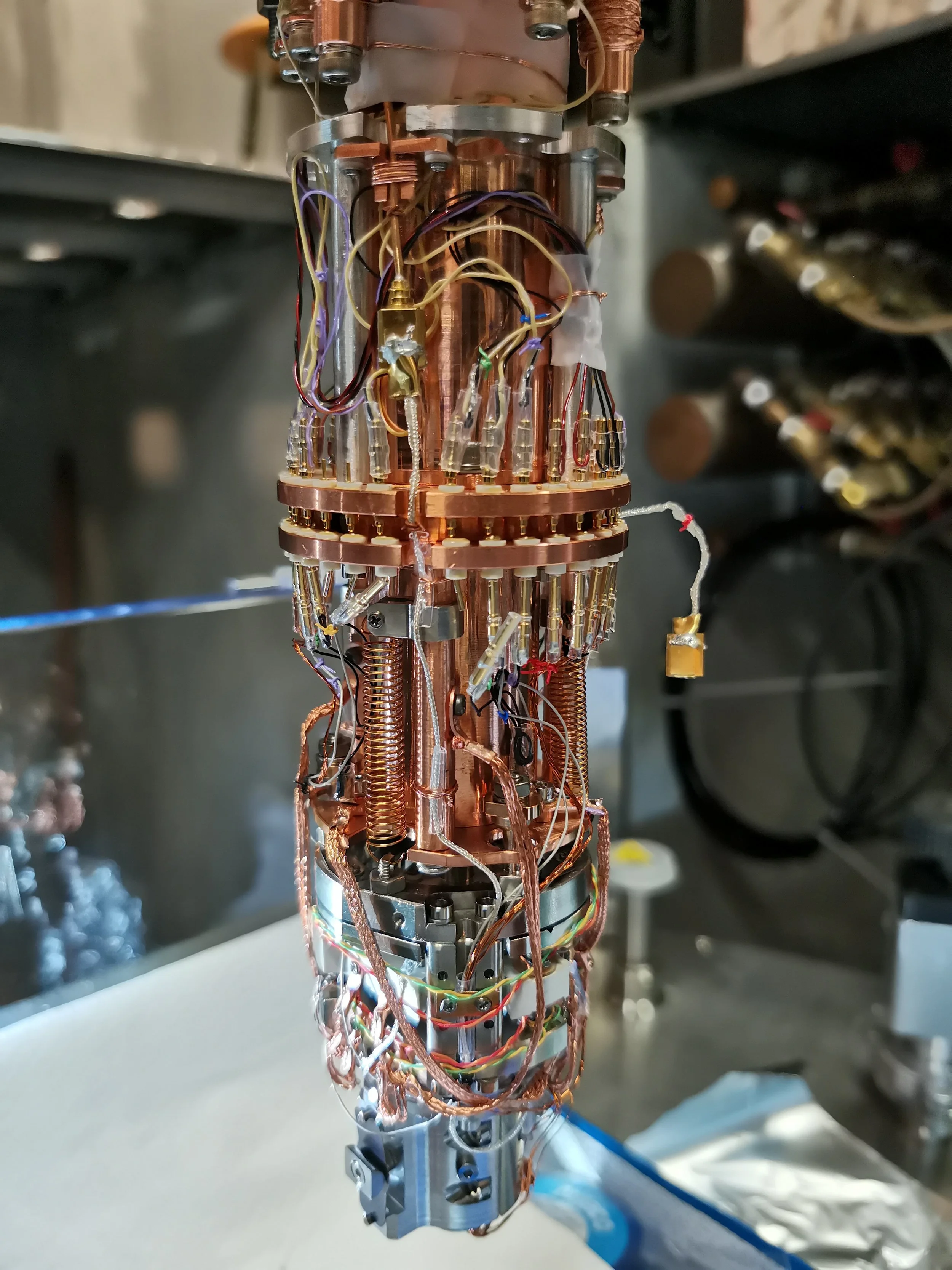
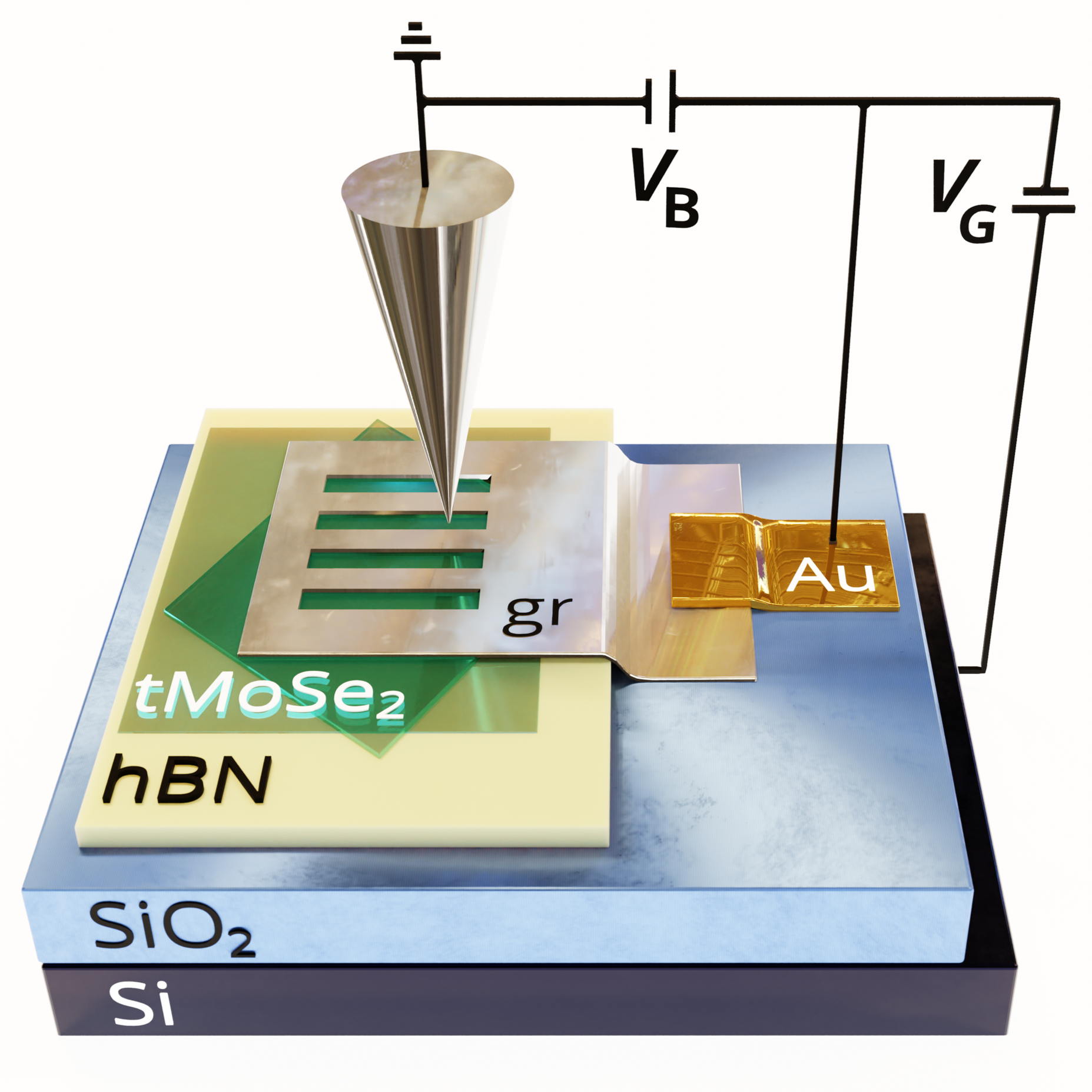
(Left) The interior of a scanning tunneling microscope, showing the dense network of electrical cables used for motorized positioning, signal readout, and device contacts. Springs and copper braids are carefully arranged to achieve sub-picometer vibration isolation while maintaining good thermal anchoring. (Bottom) An example of a gate-tunable twisted MoSe2 device fabricated for STM imaging.